


【Part 1】Clock Accuracy and Carrier Frequency Offset Experiments with the PZSDR P201Pro SDR
Introduction
When running over‑the‑air digital communication tests with separate transmit and receive SDR units, transmitter and receiver each run from their own independent reference oscillator. Even if you configure exactly the same nominal carrier frequency, physical oscillator imperfections create residual carrier frequency offset. This offset causes QAM / QPSK constellations to continuously rotate, raising demodulation bit error rates and potentially pushing offsets outside the capture range of synchronization loops.
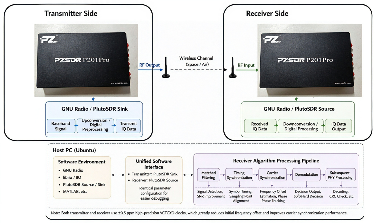
For this experimental series we set up a complete over‑the‑air test environment. We use the PZSDR P201Pro SDR for both transmitter and receiver hardware. Both sides are equipped with a ±0.5 ppm VCTCXO temperature‑compensated oscillator. This setup reduces initial carrier offset compared to setups using simpler oscillators, easing requirements for subsequent carrier‑offset estimation and carrier synchronization blocks. The hardware also supports 2×2 MIMO‑capable full‑duplex operation for future follow‑on experiments.
Figure: Block diagram of the over‑the‑air SDR test setup with dual PZSDR P201Pro transceivers
Hardware Overview
We compare key specifications between the PZSDR P201Pro and HackRF One for this experiment. Note that this comparison reflects hardware specification differences only, not subjective quality judgement.
Figure: Hardware Specs: PUZHI P201Pro vs HackRF One
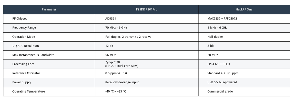
As can be seen from the table above, there is a significant gap in clock accuracy between the two devices, which is one of the key reasons for selecting the P201Pro.In addition, this device adopts an independent power supply design: industrial‑grade 8–36 V ultra‑wide input voltage (50 V absolute maximum). It delivers excellent performance with high isolation.
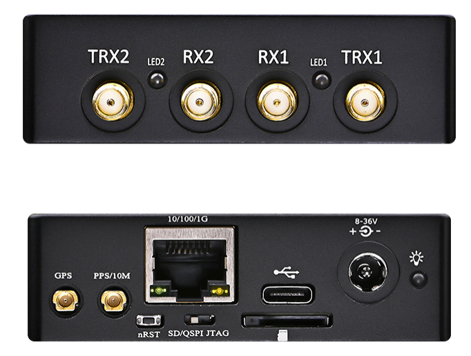
Figure: PZSDR P201Pro hardware interface diagram
Device Selection Analysis
Combined with the parameters in the table above, we further analyze the P201Pro, which is built around the AD9361.
Core Chip Differences
The AD9361 is an integrated RF agile transceiver released by Analog Devices (ADI). It integrates the RF front‑end, mixers, filters, ADCs/DACs, and digital filters into a single chip. It supports 70 MHz to 6 GHz operation, full‑duplex mode, and 2 transmit / 2 receive channels (2T2R).
In contrast, the HackRF One uses a discrete two‑chip solution: MAX2837 transceiver paired with the RFFC5072 mixer / frequency synthesizer. This is an older architecture and only supports half‑duplex operation.
Sample Bit Depth & Dynamic Range
For ADCs, every additional bit increases the theoretical quantization dynamic range by approximately 6 dB. A 12‑bit ADC yields a theoretical dynamic range of roughly 74 dB, while an 8‑bit ADC reaches only ~50 dB (calculated by the formula: \(6.02 \times N + 1.76\)).
A higher dynamic range enables the receiver to distinguish weak signals alongside strong signals simultaneously, delivering better blocking resistance and intermodulation performance, which directly impacts receive sensitivity.
Instantaneous Bandwidth
With 56 MHz instantaneous bandwidth versus HackRF One’s 20 MHz, the P201Pro can capture wider signals in a single acquisition. Examples include 20 MHz / 40 MHz Wi‑Fi signals and other wideband waveforms, leaving headroom for subsequent wideband signal processing.
Dual‑Channel & Full‑Duplex: Foundation for MIMO
MIMO systems require multiple antennas to transmit and receive concurrently, with tight clock and phase synchronization across all channels.
The P201Pro’s 2T2R architecture shares one high‑precision clock, making it naturally suited for 2×2 MIMO.
The HackRF One, by comparison, is single‑channel half‑duplex and cannot satisfy multi‑channel synchronous transmit/receive requirements.
Data Processing Core
The P201Pro uses the Zynq‑7020, featuring heterogeneous processing combining FPGA fabric and dual‑core ARM processors. Compared to the HackRF One’s MCU + CPLD architecture, it provides substantially more hardware resources for implementing complex real‑time digital signal processing.
Unified GNU Radio Software Interface
The GNU Radio integration is more consistent. Instead of the SoapyHackRF Source used previously for HackRF One, the P201Pro can connect to GNU Radio via the PlutoSDR Source block.
PlutoSDR Source offers intuitive configuration of sample rate, center frequency, gain and other parameters, simplifying receive chain debugging. The transmit side already uses the PlutoSDR Sink block. After switching the receiver to PlutoSDR Source, the transmit and receive sides share identical software interfaces. This greatly simplifies parameter tuning and follow‑up transceiver experiments.
Clock Accuracy and Carrier Synchronization
We recap the impact of clock accuracy on synchronization below.
1. Definition of ppm and Frequency Offset Conversion
ppm (parts per million) denotes the relative deviation of the crystal oscillator frequency from its nominal value. At an operating frequency of 6 GHz:
±20 ppm → Maximum frequency offset = 6 GHz × 20 ppm = 120 kHz
±0.5 ppm → Maximum frequency offset = 6 GHz × 0.5 ppm = 3 kHz
This represents a 40× difference between the two.
2. Effect of Frequency Offset on Carrier Synchronization
In digital communications, a mismatch between the receiver local oscillator and transmitter carrier frequency creates Carrier Frequency Offset (CFO). This manifests as continuous rotation of the constellation diagram and rising demodulation BER (bit error rate).
Carrier synchronization algorithms (such as Costas loops, phase‑locked loops, FFT‑based frequency offset estimation, etc.) must first "acquire" this frequency offset. Larger offsets make the loop harder to lock, slower to converge, and may even fall outside the acquisition range, resulting in loss of lock.
A high‑precision clock reduces the initial frequency offset from hundreds of kHz down to the kHz range, keeping it within the acquisition range of common algorithms. This yields more robust carrier synchronization and smaller residual frequency offset.
3. Role of VCTCXO
The VCTCXO (Voltage‑Controlled Temperature‑Compensated Crystal Oscillator) uses temperature compensation circuitry to cancel thermal drift and supports fine voltage‑controlled tuning, stabilizing frequency to the ±0.5 ppm level.
The standard XO used in HackRF One lacks temperature compensation and exhibits pronounced frequency drift with temperature variations (±20 ppm). This is one of the primary reasons stable carrier synchronization is difficult to achieve with HackRF One.
Hardware Setup
Below is a brief walkthrough of the connection procedure. While the P201Pro is a distinct hardware platform compared to PlutoSDR, it is also built upon the AD9361 at its core and streams data over the IIO interface. This enables data reception in GNU Radio using the PlutoSDR Source block.
Figure: PZSDR P201Pro physical connection
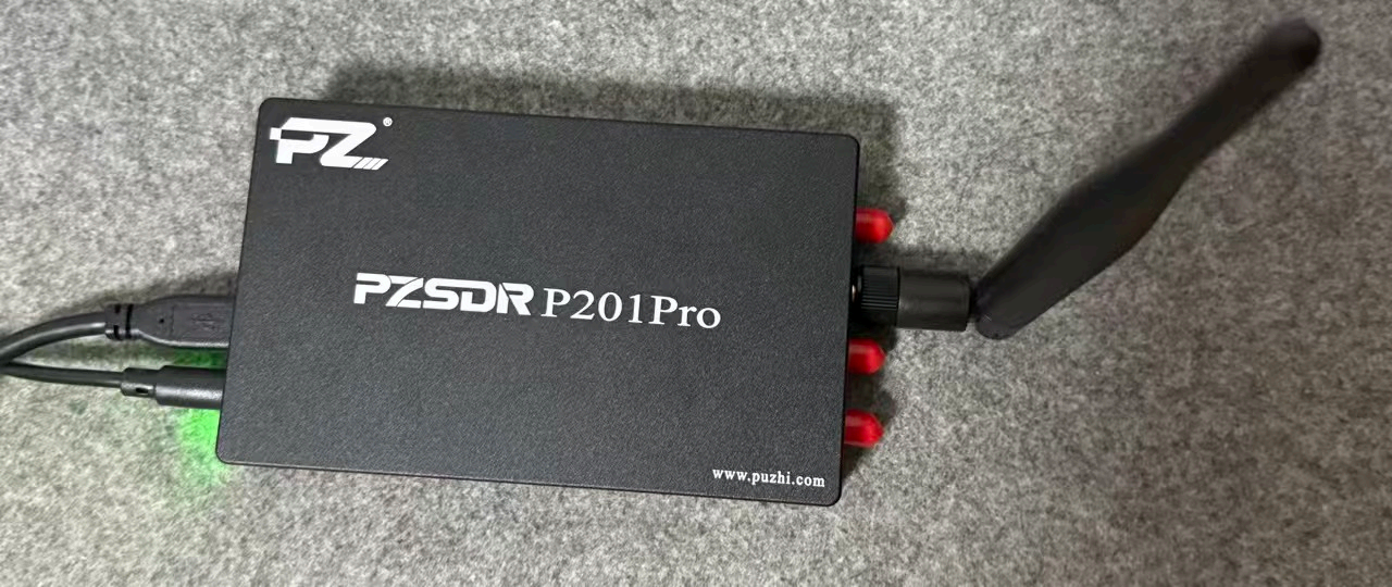
Step 1: Connect the device power cable, antenna and data cable as shown in the figure above.
Step 2: Attach the hardware to the virtual machine.
Step 3: Locate the device within Ubuntu:
iio_info -s
Sample output:
Library version: 0.23 (git tag: v0.23)
Compiled with backends: local xml ip usb
Unable to create Local IIO context : No such file or directory (2)
Available contexts:
0: 0456:b673 (Analog Devices Inc. PlutoSDR (ADALM‑PLUTO)), serial=[usb:2.18.5]
1: 192.168.2.1 (PUZHI PZSDR P201PRO), serial= [ip:pzp201pro.local]
Step 4: Launch GNU Radio.
Previously with HackRF One, the receive block was the SoapyHackRF Source. After switching to P201Pro, replace it with the PlutoSDR Source block.The IIO context URI is set to 192.168.2.1, taken directly from the terminal output in step 3.
Figure: GNU Radio flow graph screenshot showing PlutoSDR Source configuration and QT GUI visualization sinks
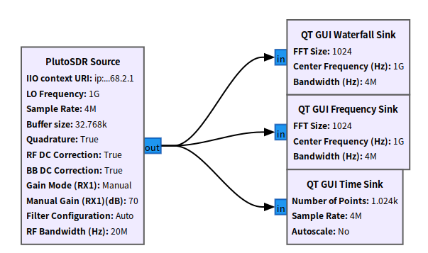
Step5: Run the flow graph configuration from step 4. Real‑time captured I/Q waveforms, spectrum and waterfall plots will be displayed to confirm successful hardware reception.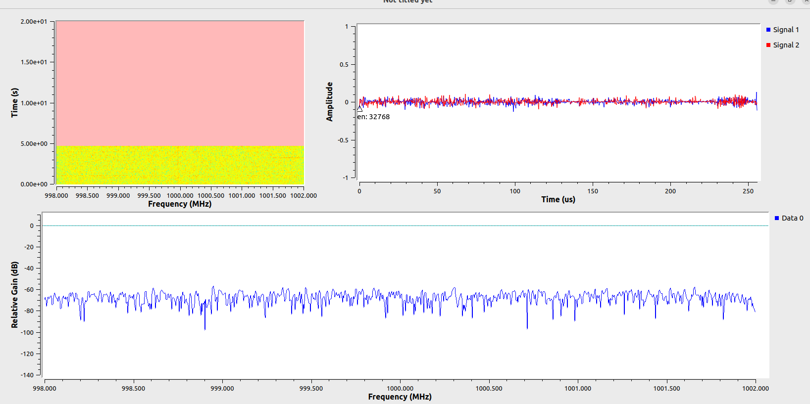
Figure: GNU Radio runtime screenshot showing captured spectrum, time‑domain I/Q samples and waterfall output
This confirms successful device connection. At this point, the receiver‑side hardware upgrade is complete. All subsequent experiments will use this platform.
Summary
Reference oscillator performance is a frequently overlooked but critical factor for over‑the‑air digital communication SDR experiments. Oscillator PPM error directly translates into carrier frequency offset which increases the difficulty of carrier synchronization.
Hardware with high‑performance VCTCXO can constrain initial offset to within the practical capture window of common GNU Radio carrier recovery blocks.
In the next part of this series we will move on to practical QPSK reception, observing how Costas loop carrier synchronization works on real‑world over‑the‑air captured signals.
Leave us a message
Puzhi focuses on SDR and ARM/FPGA technology solutions