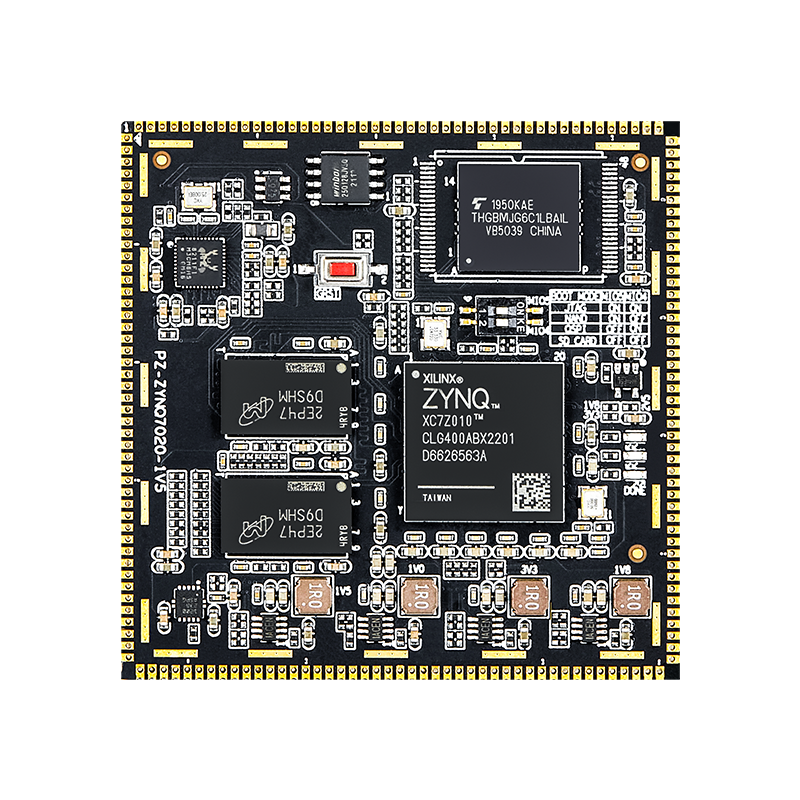
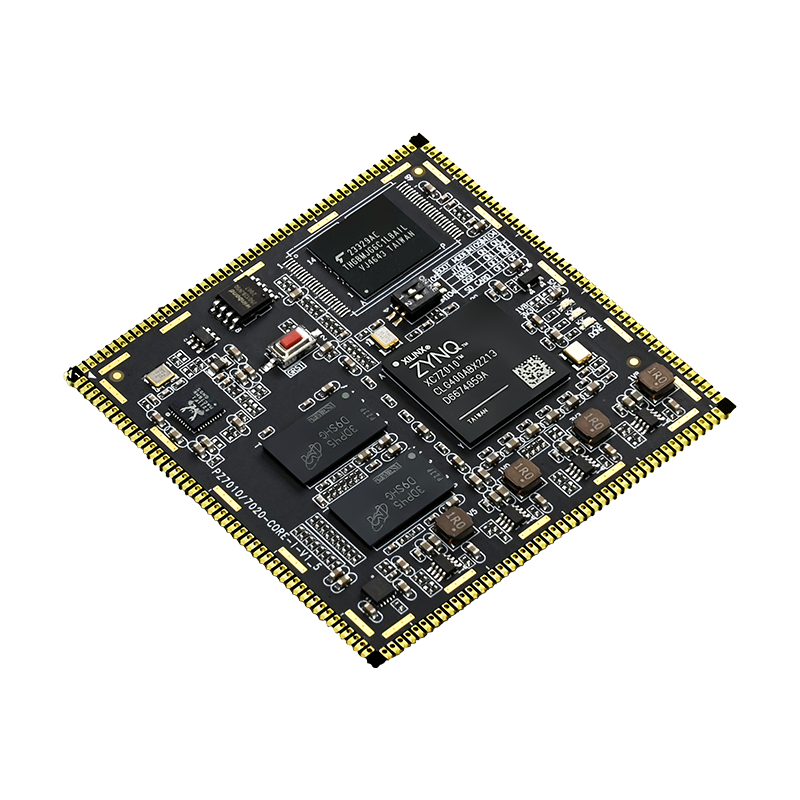
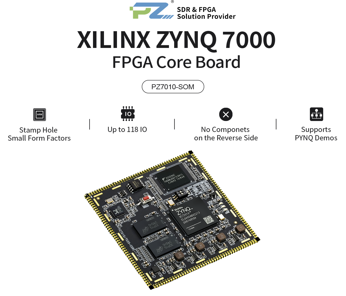
Puzhi FPGA ZYNQ7000 ZYNQ7010 Core Board
- ZYNQ core board,dual-core ARM Cortex-A9,main frequency 667Mhz
- 512MB DDR3,4GB EMMC,128Mb QSPIFLASH
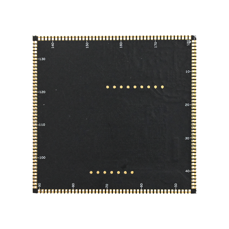
- Small size 61mm*61mm,up to 118 IO available,no components on the back
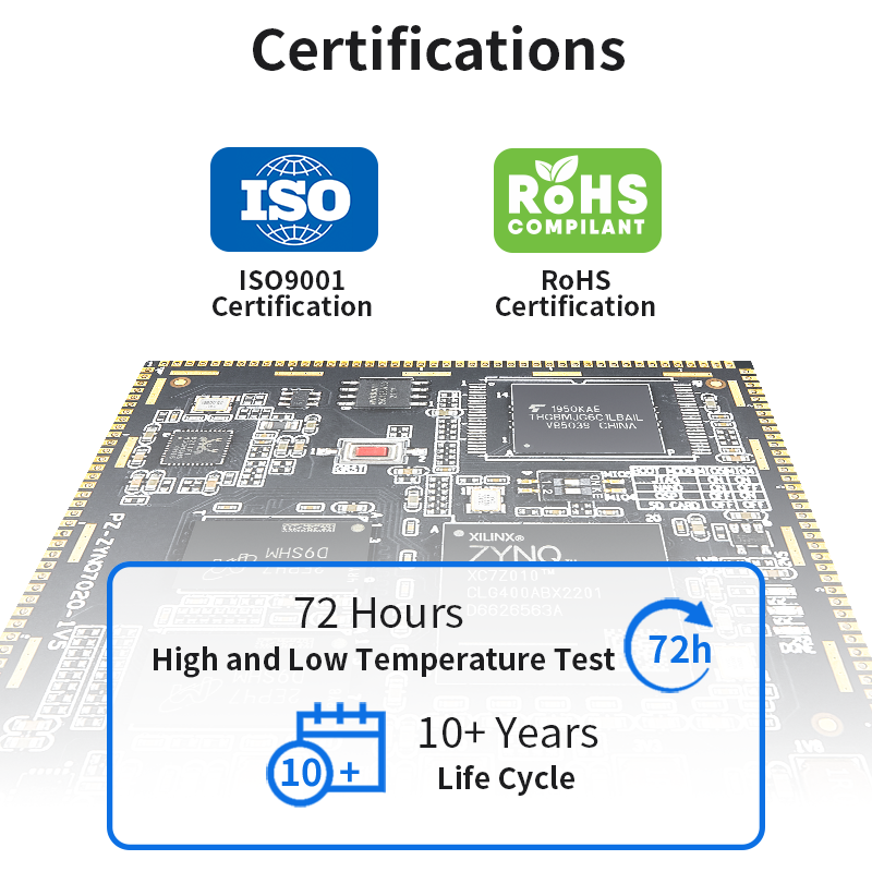
- Extreme material selection and process standards,industrial grade -40℃~+85℃
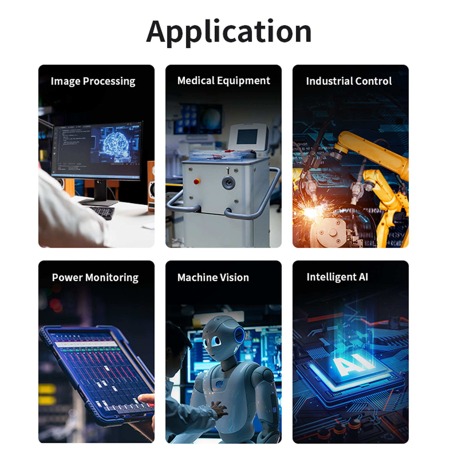
- Support PYNQ,provide hardware reference & rich routines,help product development
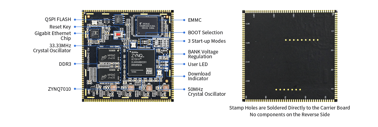
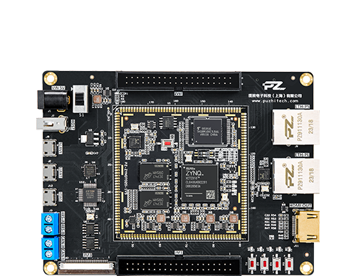
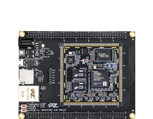
Interface Function Display
What is the benefits of stamp hole design in ZYNQ 7010 Core Board?
1. Efficient production and assembly
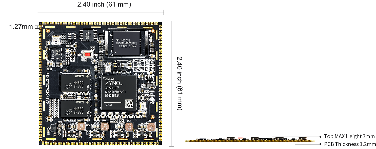
The small-sized stamp holes enable multiple small-sized PCBs to be assembled onto the substrate for mass production. They can be easily separated by simply snapping or cutting, significantly enhancing production efficiency and reducing costs.
2.Modular design is flexible
In high-density PCB design, the small-sized stamp holes allow for the quick assembly and disassembly of independent modules (such as sensors, power management, etc.), facilitating maintenance and upgrades.
3.Stress dispersion and reliability
The circular or elliptical hole design of stamps can avoid stress concentration during plating, reduce the risk of damage to circuits and components during plating, and improve the flatness of the edge of the board.
4 Electrical performance guarantee
The small-sized stamp holes are designed with a reasonable spacing (usually 1.5-3mm), which not only ensures the stability of current transmission but also prevents solder short circuits or poor component contact. It is suitable for high-precision circuit connections.
Remarks :Small-sized circuit board stamping holes (From 0.8 to 1.2 mm)
Product Parameters
ZYNQ7000 ZYNQ7010 -SOM FPGA Chip XC7Z010-2CLG400I Specification
FPGA Core Board | PZ7010-SOM |
FPGA Chip | XC7Z010-2CLG400I |
Processor Core | Dual Core ARM Cortex-A9 |
Speed Grade | 2 |
Chip Level | Industrial Grade(-40°C~+85°C) |
Logic Cells | 28K |
Lookup Tables | 17600 |
Flip-Flops | 35200 |
DSP Slices | 80 |
BLOCK RAM | 2.1Mb |
DDR3 | 512MB |
QSPI FLASH | 128Mb |
EMMC | 4GB |
PS Side MIO | 24 |
PL Side IO | Total 94 Single-ended IOs of which, 46 IOs fixed at 3.3V,48 IOs 1.8/2.5/3.3V adjustable,default 3.3V |
Start-up Mode | JTAG/QSPI/SD, On-board DIP Switch Selection |
Gigabit Ethernet | 1 |
User LED | 2 |
Voltage/ Current | 5V/1A |
Crystal Oscillator | Single-ended Crystal 33.3333MHz for PS Single-ended Crystal 50MHz for PL |
Core Board Form Factors | 2.40 inch x 2.40 inch (61mm x 61mm) |
Product Dimensions
Product Packages
Technical Support
Contact Customer Service after Purchase Files Saved in Google Drive/ Yandex/ Dropbox

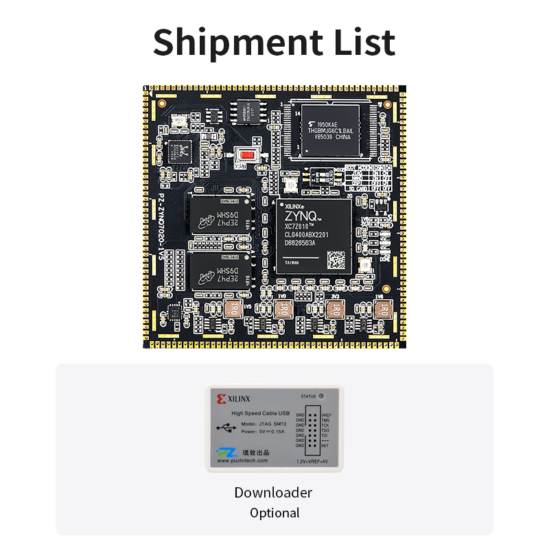
Standard Delivery List

1. Demos Come with the Board
2. Professional technical engineering team online support
 After-sale Service
1. The Guarantee Period Amounts to one (1)Year after Delivery ofthe Products
2. Be careful not to Connect the Wrong Power Supply, Pay Attention to Anti-static.
3. Dealer Discount, Send Email for Quotation and Lead Time. Technical Email: support@puzhi.com
4. Documents provided accordingly,saved in the Google Drive/Yandex/Dropbox Contact Sales person to Get it after Purchased.
 Documents & Shipment
1. QT/PI/CI/PL/BL and relevant documents for customs clearance
2. DHL/DPEX/EMS/E-EMS/ Fedex lE/ Fedex IP/ SF Express/ UPS, 3-7 working days will reach you
3. If order large quantity , Air or Sea transportation can be negotiated Trade terms & Payment methods
1. EXW/FOB/CNF/CIF/CFR/FCA/CPT/CIP
2. TT/LC/ Paypal/Western Union/Ali-express/Master/Visa
Leave us a message
Puzhi focuses on SDR and ARM/FPGA technology solutions